Mastering AXI
Implementing an AXI4 master in SystemVerilog.
I recently created an AXI master for a RISC-V CPU I am working on at my university. In this post, I'll share the details of how such a component works; in a way that even someone completely unfamiliar with AXI can fully understand the implementation.
This is important because FPGA systems (especially Xilinx) often use AXI to interface with ready-made components. Because of that, moderately complex designs will almost always have something AXI-related - it will surely come up at some point.
GitHub repo
The code shown here will be somewhat simplified, omitting some details that are important for our project, but that wouldn't bring value to this post. With that out of the way, the code of the module used in production is available on GitHub.
If you think something is missing in the code provide here, take a look at the module source.
What even is AXI?
AXI is a point-to-point on-chip communication bus protocol. In more human terms, it is one way in which separate components inside a computer chip can talk to one another. Point-to-point means that it describes the communication between exactly two components - a Master and a Slave. The Master is always the one to initiate communication by either saying "Take this data!" or "Give me that data!", the slave only does what it is told.
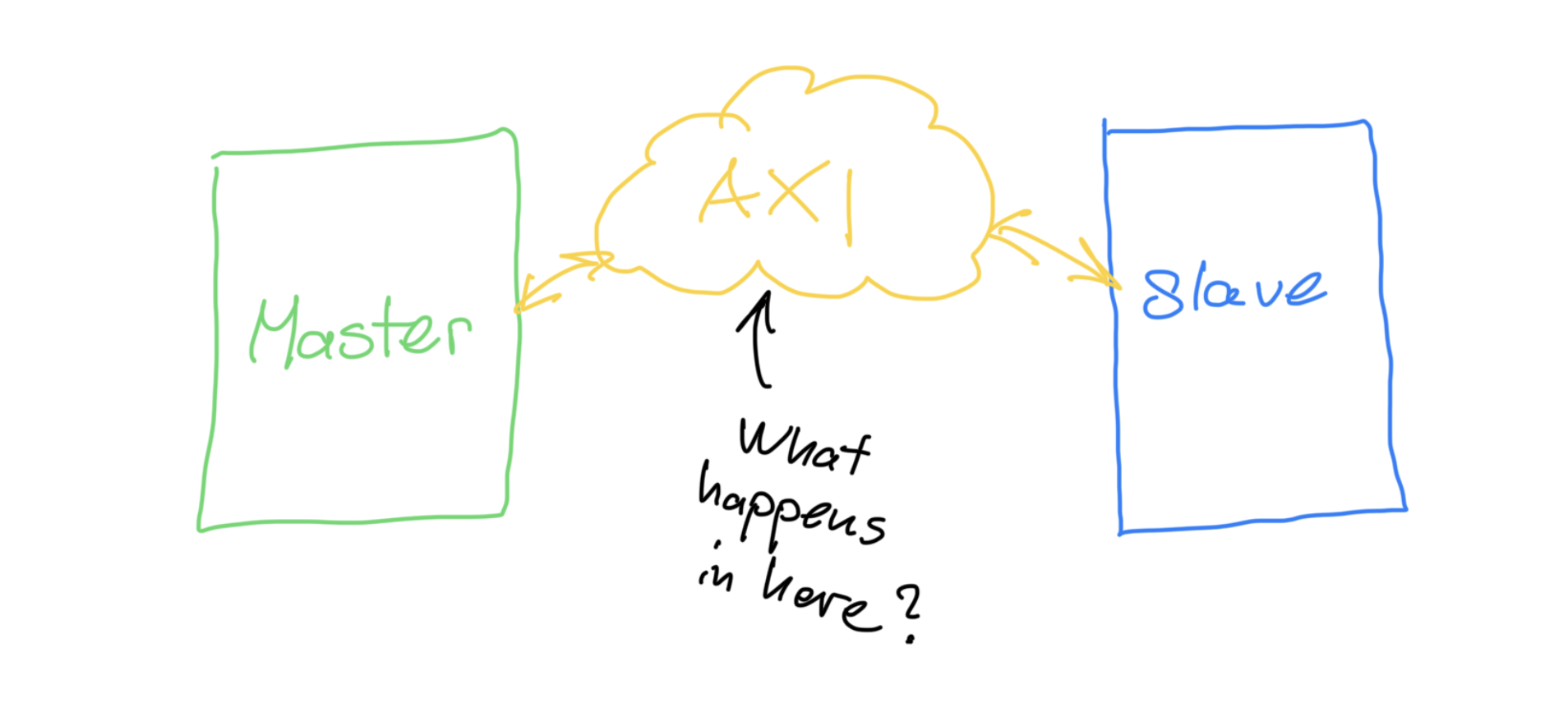
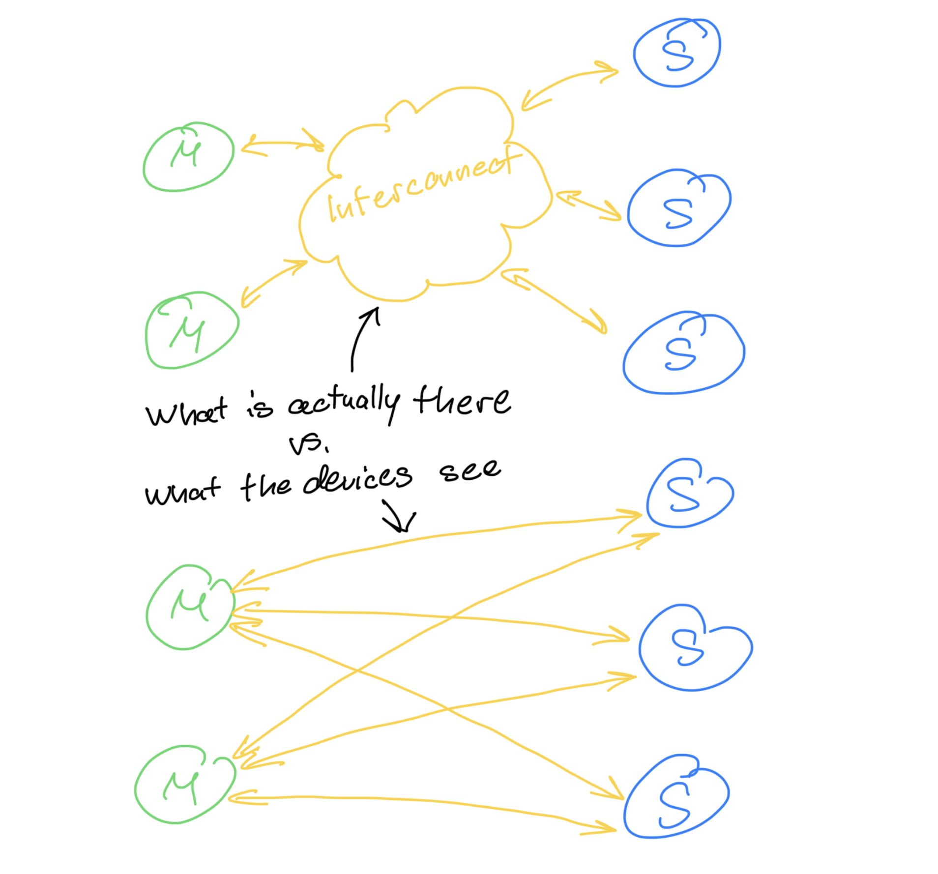
As exactly one Master talking to exactly one Slave wouldn't necessarily be useful, special switches called interconnects are used to connect multiple Masters to multiple Slaves in a transparent way - their communication happens as if it was point-to-point. We won't talk about interconnects much from this point forward - their inner workings are complex and comparable to black magic - just know that they exist and that many Masters and Slaves can be connected into an AXI network**.
How AXI works
Each Slave on a network has an assigned address (or range of addresses) by which it is identified. An interconnect knows which Slave a Master is trying to reach because the Master told it the address of the Slave it is trying to reach.
A unit of communication is called a transaction. It can be either Read or Write. So what a Master is doing is saying "I need to read data from (the slave at) address X." or "I need to write data to (a slave at) address Y."
After that, the slave answers with either "Here is your data, all good!", "Great, I got the data!", or "Nah, something is wrong."
We see that each transaction consists of an address, data, and a response. In AXI, these are different channels between the Master and Slave.

But wait, why is there a Write Response channel, but no Read Response channel? A channel is a one-way communication line. The direction of the Read Data channel is from the Slave to the Master - the response can be sent together with the data! With reads, that is not possible, as the source of write data is the Master, not the Slave.
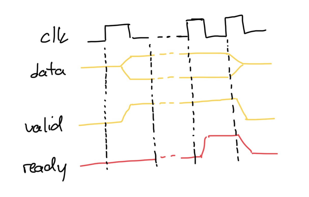
Now that we understand what are the parts of an AXI system, the last piece of the puzzle we need before diving into the implementation is the way in which information is passed around through the channels.
In AXI, when a source wants to send a piece of data, it must also tell the destination that the data is valid (i.e. there is some data inside the channel), and it must keep that data on the bus until the destination is ready to receive it. That naturally means that each channel will have three lines - a data bus, a valid line, and a ready line.
Such sending of a single piece of information from a source to destination is called a transfer.
Let's now put that all together - to complete a transfer, the source puts data on the data bus, sets the valid line high, and waits for the destination to read the data. Once the destination has read the data, it sets the ready line high. The transfer has now completed.
There are many other control and option signals, too, but these are not that importat right now and we will touch on a handful of them later. There is a list of them on Wikipedia. In this post, I am primarily writing about AXI4, but there is a "slimmed-down" subset of it - AXI4-Lite - with only the necessary signals. As AXI4-Lite doesn't have all the features my project requires, I needed to implement AXI4-Full, so that is what we are discussing here.
A transaction consists of a transfer of the address from the Master to the Slave, one or many transfers of data, and the transfer of a response. The last piece of data is always marked with a last signal. We are only implementing the ability to transfer single pieces of data at a time (single-beat), so data will always be marked as last.
Let's look at two more hand-drawn waveforms and jump into SystemVerilog after that.
The first is a full write transaction, here shown without waiting - i.e. completing in the smallest number of cycles possible in this implementation.
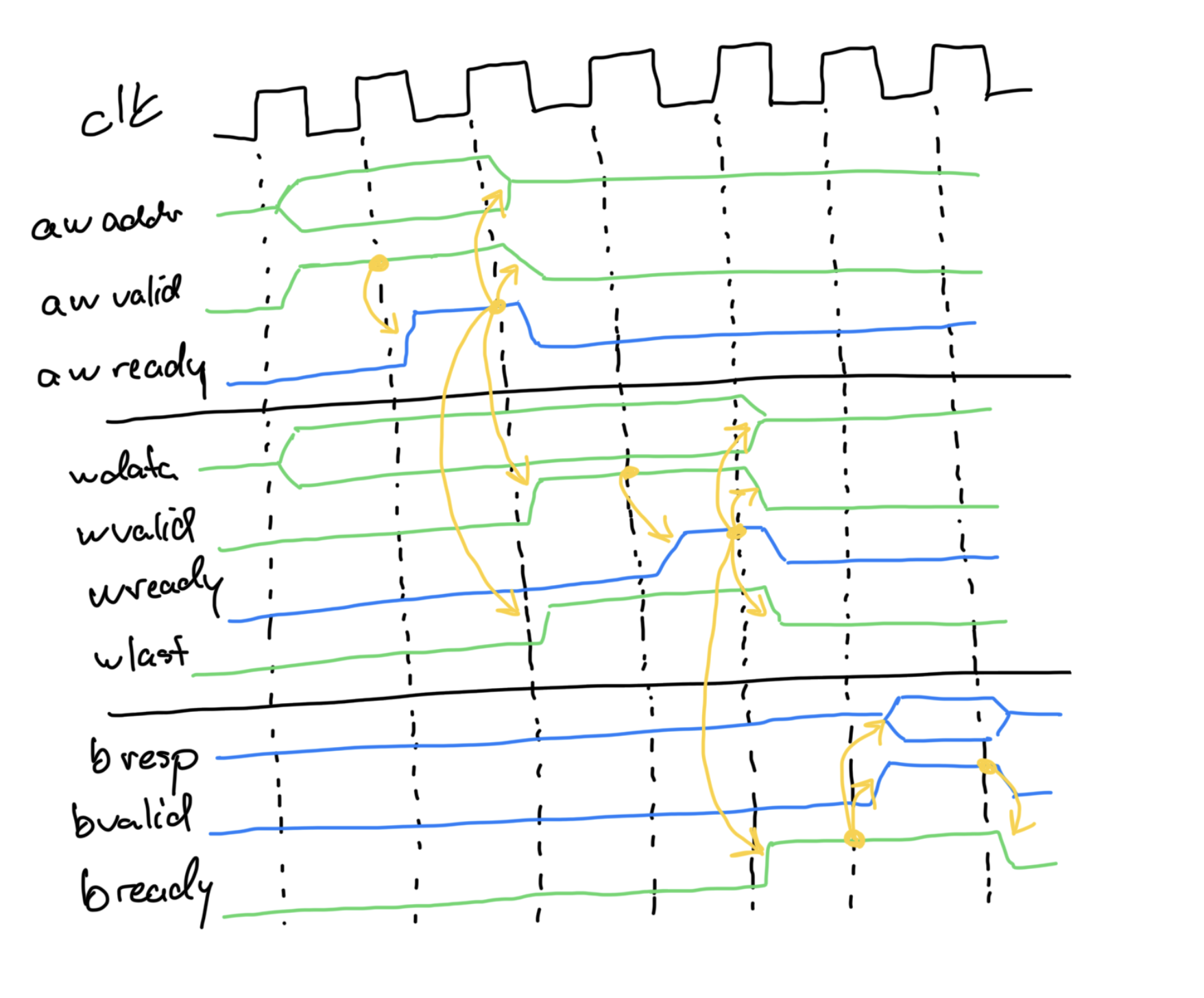
Notice that data becomes valid when the address is received, and that the Master is ready for the response as soon as the Slave receives data.
Now onto reads - this is simpler.
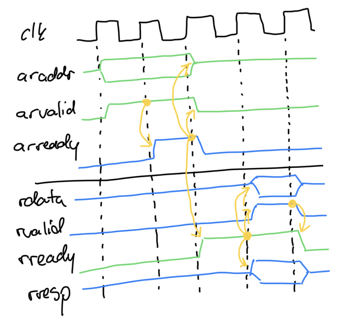
The address is set in the same way, and the Master is ready for data and response as soon as the address transfer completed. When data is valid, the master can read it and set ready high, completing the transaction.
Writing the code
Timing doesn't have to look exactly like that, but we will be implementing it that way. If you want to find out more, I recommend reading ARM's AMBA AXI Protocol Specification.
I implemented this in SystemVerilog, but other HDLs should be similar. SV is what I am most comfortable with, and SV is what we are using for the project. We will start by first defining an interface, then go on a brief but important digression about timing,, and then finish off with implementing it in SystemVerilog
Interface
Aside from the AXI signals discussed above, our Master needs an internal "host" bus which will be interfacing with AXI. Essentially, our module translates host bus requests to AXI transactions.
The host can read and write data from/to an address. While a transaction is in progress, it needs a wait signal. When wait goes low after a transaction was initiated, the host knows that the data was written successfully, or that it can take data that has been read.
Additionally, AXI supports 32- and 64-bit data. We will require it as the WIDTH parameter and come back to it later. AXI addresses are always 32-bit, so we don't need an ADDR_WIDTH param.
That leaves us with this interface:
module axi_master #(parameter WIDTH = 32)(
    input  logic             i_clk,
    input  logic             i_rstn,

    // Host bus

    input  logic [31:0]      i_addr,   // Address bus
    input  logic [WIDTH-1:0] i_wdata,  // Write data bus
    output logic [WIDTH-1:0] o_rdata,  // Read data bus
    input  logic [1:0]       i_rw,     // 00-idle, 01-write, 10-read
    output logic             o_wait,   // Transaction active

    // AXI signals

    // Write Address (AW) channel
    output logic             m_axi_awvalid,
    input  logic             m_axi_awready,
    output logic [31:0]      m_axi_awaddr,
    // And so on...
);
Note: My convention is to mark inputs as i_, outputs as o_, registers as r_, wires as w_ and states as S_. By Xilinx convention, AXI Master signals are prefixed with m_axi_ (and Slave signals with s_axi_).
There are additional control, status, and debug signals in the GitHub code, we will be ignoring these here.
Internal timing
As discussed, this Master is essentially an FSM - based on inputs and the current named state, it determines outputs and the next named state. Moreover, it is a Mealy FSM, outputs are calculated combinatorially, and as such are available on the following rising edge of the clock. That is important because a module connected to the Master can expect results when the rising edge comes. If it was a Moore machine, outputs would update on the following rising edge.
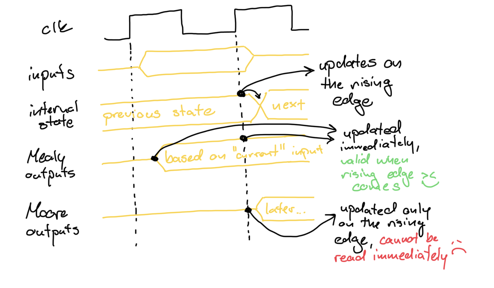
As you can see, the state machine needs to "predict" the next state based on the "previous" state and the current inputs. The outputs will look as if the transition happened immediately, when in reality the "actual" state was only updated later. That is how we achieve a zero-cycle response.
We want the state to update on the rising edge of the clock, and outputs to update immediately. Naturally, that requires an always_ff block for the clocked logic, and an always_comb block for the combinatorial logic.
This implementation will capture inputs on the start of the transaction, and register outputs after it has finished. That means that the host can request the transaction and release inputs immediately, with the Master "remembering" them - storing them in internal registers for the duration of the transaction. Similarly, read data will be registered on the output. The host can then read it whenever it wants, but before starting the next transaction (and overwriting it).
To get that captured-inputs, registered-outputs behavor, we will need some internal registers, as well as a state register, with fitting names.
// Internal signals
state_e r_state;
state_e w_next_state;

logic [31:0]      r_addr;
logic [WIDTH-1:0] r_wdata;
logic [WIDTH-1:0] r_rdata;
logic [1:0]       r_rw;

// Clocked logic
always_ff @(posedge i_clk) begin
    if (!i_rstn) begin
        r_state <= S_IDLE;
        r_addr  <= '0;
        r_wdata <= '0;
        r_rdata <= '0;
        r_rw    <= '0;
    end else begin
        r_state <= w_next_state;  // Always register the next state

        // Capture inputs if a transaction was requested
        if (r_state == S_IDLE && i_rw != RW_NOP) begin
            r_addr  <= i_addr;
            r_wdata <= i_wdata;
            r_size  <= i_size;
            r_rw    <= i_rw;
        end

        // Register read data when valid
        if (m_axi_rready && m_axi_rvalid) begin
            r_rdata <= m_axi_rdata;
        end
    end
end
Notice that w_next_state is a wire! It is calculated combinatorially and registred into r_state on the rising edge of the clock...
A transaction starts when no other transaction is active (state is S_IDLE), and a transaction is requested (the requested operation i_rw is not no-read-write-operation RW_NOP). The next state will be calculated combinatorially and already present in w_next_state, so clocked logic only needs to capture inputs (zero-cycle response)!
The first if statement handles capturing inputs, the second if statement handles registering outputs - more precisely, if there is valid data on the read channel (m_axi_rvalid), and we are ready to read the data (m_axi_rready), then we can actually read the data - i.e. put it on the host bus.
State machine
Now we will go through the actual state machine. There is probably a million different and completely valid ways to accomplish this, and this is just one of them which I came up with. It is in no way the-only-way-to-create-an-AXI-master, so I won't go into too much detail. The general idea is more important here.
Coming up with a state diagram out of thin air can sometimes be challenging, so we will follow the write path first, then the read path, and mark important actions along the way. Here I will show code immediately, but in practice the entire state machine will be designed first. Either way, I believe this will be more understandable.
As we discussed above, the outputs and next state need to be calculated combinatorially - i.e. in an always_comb block. All outputs must be set in each code path, so we will set them to default values just to be sure.
After setting default outputs, we will reassign them based on the current state in r_state. A natural way of implementing this is a case block. As we will be specifying all possible values that can be in r_state, we can use a unique case block and forego the default case.
We can also assign addresses to be constant and address valid to depend on the state.
// Combinatorial logic
always_comb begin
    // Default actions
    w_next_state = r_state;           // Keep current state
    o_wait       = r_state != S_IDLE; // Wait if not idle
    // No valid data on AXI, and not ready for any data
    m_axi_wvalid = '0;
    m_axi_wlast  = '0;
    m_axi_bready = '0;
    m_axi_rready = '0;

    m_axi_awaddr = r_addr;
    m_axi_araddr = r_addr;

    unique case (r_state)
        // Stuff from below goes here!
    endcase
end
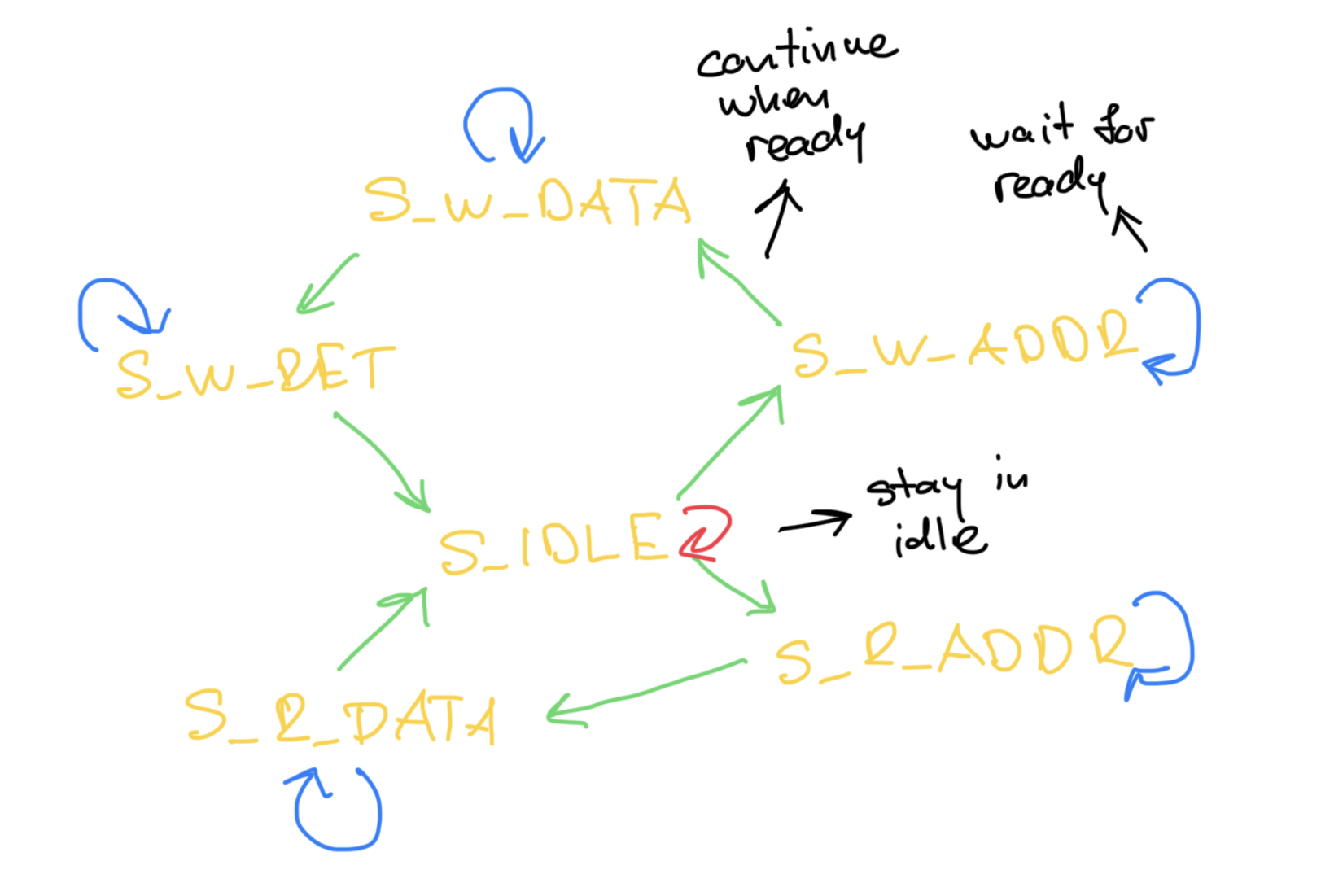
Let's start with writes - we will obviously start with no transaction active, so we have a "not doing anything" state. Let's call it S_IDLE. When in S_IDLE, nothing is on AXI and the Master is waiting for the host to request a transaction.
Once the host wants to start a transaction, we need to determine whether it is a read or a write. If it is a write, we go onto the write path, and if it is a read, we go onto the read path. We know the first actions for both - setting the address on their respective channels (Write Address - axi_aw or Read Address - axi_ar).
Let's name those states S_W_ADDR for writes and S_R_ADDR for reads and continue with the S_IDLE case. If a transaction is started, we need to assert the wait signal to tell the host that we are (still) processing the just-requested transaction. Remember - this needs to be combinatorial because the signal needs to be valid when the clock comes.
S_IDLE: begin
    // A transaction is requested
    if (i_rw == RW_WRITE || i_rw == RW_READ) begin
        // Set next state based on i_rw
        w_next_state = (i_rw == RW_WRITE) ? S_W_ADDR : S_R_ADDR;
        // We want wait high immediately
        o_wait = 1'b1;
    end
    // If no transaction is requested
    // Default assignments cover us here
    // Stay in the same state with nothing on AXI and wait low
end
Going onto the write path, we need to set the address, and continue to setting data only when the address was confirmed by the Slave. This complicates things a bit, but this is still by far the simplest case. If Write Ready (m_axi_awready) is low - the Slave didn't read it yet, stay in the current state. If it is ready, go to the next state.
The next state is setting data, so we will name it S_W_DATA.
S_W_ADDR: begin
    w_next_state  = (m_axi_awready) ? S_W_DATA : S_W_ADDR;
    m_axi_awvalid = 1'b1;  // Address is valid
end
Now we are setting data. That means that there will be valid data on the bus. Similarly to the last case, if we get the ready signal, we move on to the next state. If not, we stay in the current state. We also need to keep in mind that this is the last data transfer (since we are only doing single transfers).
The next action involves returning the response, so let's call it S_W_RET.
S_W_DATA: begin
    m_axi_wvalid = 1'b1;
    if (m_axi_wready) begin
        w_next_state = S_W_RET;
        m_axi_wlast  = 1'b1;
    end
end
Lastly, we do a similar handshake on the Write Response (axi_b) channel, although this time it is a little different. That is becasue now we are receiving data, not sending it - ready and valid are flipped.
We say that we are done - i.e. set o_wait low, and go into an idle state after getting a response.
S_W_RET: begin
    m_axi_bready = 1'b1;  // We are READY, not VALID
    if (m_axi_bvalid) begin
        w_next_state = S_IDLE;
        o_wait = 1'b0;
    end
end
And we ended up in the S_IDLE state again! Now onto reads.
This is even simpler as there is no response, and we already covered all of the concepts already. Starting with the address state S_R_ADDR, it is identical to the corresponding write state, just on the read channel.
S_R_ADDR: begin
    w_next_state  = (m_axi_arready) ? S_R_DATA : S_R_ADDR;
    m_axi_arvalid = 1'b1;  // Address is valid
end
After that we read the last piece of data in the S_R_DATA state, setting o_wait low when valid, after asserting we are ready for data.
S_R_DATA: begin
    m_axi_rready = 1'b1;
    if (m_axi_rvalid) begin
        // Idle immediately, no waiting for response
        w_next_state = S_IDLE;
        o_wait = 1'b0;
    end
end
At last, we can show the state diagram:
"But wait", you must be thinking "where is o_data set?!" And you would be right to question that - I left it for the end because it requres understanding both the timing and the state structure.
It is assigned combinatorially at module level, switching between the data straight from the bus and the registered data. If you recall, registered outputs are only available after the clock cycle. That means that if the host was checking if o_wait was low on the rising edge - and it was - it would get the previous registered data, as the new read data is being registered at that moment (look at the last timing diagram).
Because of that, we want to combinatorially set o_rdata when it is valid on the bus, and o_wait will be low on the following rising edge. That leaves us with this assignment, saying "If read data (m_axi_rdata) is valid (m_axi_rvalid), output it as o_data, otherwise output the previously registered value (r_rdata)":
assign o_rdata = (m_axi_rvalid && m_axi_rready) ? m_axi_rdata : r_rdata;
Note that the code shown here is significantly simpler than the production code in the GitHub repo. That is because that module reports error status and can handle variable width inputs by shifting bits. The implications are that the host wouldn't know of any errors happening on AXI (instead seeing a transaction completing normally with o_wait going low), and more importantly, data can only be exactly as wide as AXI is - if it is 32-bit AXI, all data is 32-bit (WIDTH=32), and if it is 64-bit AXI, all data is 64-bit (WIDTH=64). If you are interested in that implementation, take a look at the GitHub code.
Conclusion
AXI is a complex protocol used in many real-world systems and crucial in FPGA-based designs. Here we implemented a bare-bones master with a minimal set of features required to communicate with "real" AXI devices.
Overall, this implementation would be quite inefficient in an actual system, thanks to doing single transfers per transaction, but it serves as an educational example and a good starting point for implementing a more robust master.